All about PCB Design
Saturday, 18 October 2014
Monday, 13 October 2014
What is a latch mode in Pulsonix PCB Design tool?
Latch mode is a mode of operation that allows a tool to be pre-selected (latched) and applied to many
items until it is toggled off (unlatched). For example, the Rotate mode can be latched down and
rotations applied to many components in the design in turn.
To exit latch mode, you can either select the option again to unlatch it, or press the Esc key on the
keyboard to return to Select mode. You can also use the Cancel option from the context menu after
right clicking the mouse.
How to enable / disable Status Bar and Workbook mode in Pulsonix PCB Design tool?
Status Bar
Is really cool feature. In that window you can see in what mode you are active. You can toggle in between the Units ( by just double click at mm or thou ). It also display tips as well as co-ordinates.
You can enable or disable this feature from View > Status Bar
Workbook mode is show you all those pages you have opened in Pulsonix PCB Design tool. As you can see in above image ( Schematic , PCB , footprint and symbol )
To toggle in between shortcut key is ctrl +Tab
If you are not happy with its location then you can move it to the top.
Select " Customize" from " tools " menu and then go to " Application Look " and make changes
To enable or disable this feature go to view > Workbook mode
Saturday, 11 October 2014
What is a Via, Micro via, buried via and blind via in PCB design?
Via
In PCB Design a via made an electrical connection between two or more layers. Its visible from both side of PCB.
Yes, its more like a Pad which has a drill hole. But drill dia for Via is smaller as compare to Pad. And that is the only part which distinguish it form Pad.
Blind via
It's start from one of the surface to any of inner layer.Burried Via
It's via that is between inner layers. burried via is not accessable from top or bottom layer.Microvia
These are the vias with narrow drill hole. usually these vias are directly present in component pads.
Reference:-
- Reduce Your PCB Costs With Blind Vias, Buried Vias & Microvias Retrieved on 11 Oct 2014 http://www.eetimes.com/author.asp?section_id=36&doc_id=1320862
How to change Solder Mask in Pulsonix PCB Design tool?
Problem:-
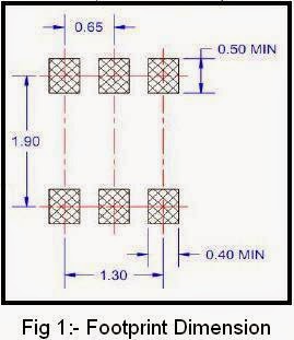
I have to creat a footprint as shown in Fig 1. But after creating ( see Fig 2 ) I got my Solder Mask connected. I would like to get clearance in between the Solder Mask. Please tell me solution for this. I am using Pulsonix PCB Design tool.
Solution:-
To fix this you need to make change in Technology file.
- Select " Technology " from "Setup" menu or press T key
- On your right side select Layer Classes
- Then click on " Solder Mask " > Edit
- Change the value in section " Pad Oversize" to 2 mil. Make sure you are working in "thou".
Exit from window by pressing OK. Your mask will change and will look like as shown below.
In Pulsonix you can change Pad numbering quick to learn that trick click here
How to add pad number fast and Automatic in Pulsonix PCB Design tool?
In Pulsonix PCB Design tool while creating footprints you can assign PIN number Automatically or manually but really really fast.
Steps for manually Pin numbering
Steps for manually Pin numbering
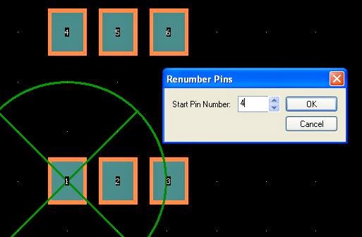
- Select " Renumber Pins" from "Utilities" menu
- And select your numbering from where you want. In this case ( according to below image ). I need to make changes from Pin number 4. So I just enter 4 and click OK.
- Then I will click the right top Pad first and then will move further left and at last click any where in black window. And you are done.
Steps for Auto Pin numbering
- Select " Renumber Pins" from "Utilities" menu
- Then " Check by location "
- In sides you select both sides
- In Direction you select Left to right and bottom to top
- Your numbering are in reverse. So, here you select " Alternate Directions"
- Make sure you check for "reverse left - right on bottom side"
- Then Click OK
- A notepad will popup and will show you what changes has been done.
- Below image showing your Pin number as per datasheet.
How to add two planes in Inner layer for Ground and Power for Pulsonix PCB Design tool?
Demonstrated on
Pulsonix Version 8.0
OS XP SP3
i3 Processor 2GB RAM
4 Layer PCB Board
- Signal TOP
-gnd Inner 1
-power Inner 2
-Signal BOTTOM
Pulsonix Version 8.0
OS XP SP3
i3 Processor 2GB RAM
4 Layer PCB Board
- Signal TOP
-gnd Inner 1
-power Inner 2
-Signal BOTTOM
Friday, 10 October 2014
How to add copper layers for ground and power inner layers in 4 layer and more PCB design case. Need solution for Pulsonix PCB Design tool.
In Pulsonix we do it with Copper Pour. ( with the help of template option in insert menu )
If a copper area is to be inserted without the need for voids around unconnected tracks, components,
pads, etc then use Insert Copper facility.
Demonstrated on
Pulsonix Version 8.0
OS XP SP3
i3 Processor 2GB RAM
4 Layer PCB Board
- Signal TOP
-gnd Inner 1
-power Inner 2
-Signal BOTTOM
Moving forward. To do so first you create a template and then from the utility open pour copper and you done.
But there are some if and buts which you need to control and modify.
First thing you do before pouring or getting your copper layer. Setting up the Technology for this option.
4. You make settings for Thermal Rules and Copper Pour as per your requirements. Shown are default settings.
5. May be you would like to do some more. One more is in Design Setting.
6. Setup > Design Setting or press shortcut key " Shift + D"
7. Look for "Template" on right side. Refer below image
8. Next setting you do is how you prefer to add copper. For that there is one more setting.
9. In tools > Options [ shortcut key " O "
10. look for "Interaction" on right and make your setting, refer below image.
11. You will see two options
a) Act Poured:- In this option you add " pour copper" latter from Utilities menu.
b) Pour On Add :- In this option as soon as you done with template. Area will get filled with copper right away.
To start the copper plane.
You go to Insert > Template and pick your desire option ploygon, rectangle, circle , line
Then start drawing it, when you done
As you can see in above image I have got my template (polygon) in golden colour. And dark green is my Board outline outline.
To Assign net name to the plane / template. Select any one side of template ( in above image is in light green colour) then right click on it > Net > Change Net ( or simply Press " F2 " on your keyboard ).
Change Net window will appear from the drop down menu you will be able to select your desired net and then press OK.
Click at " Pour Copper" from Utilities
If a copper area is to be inserted without the need for voids around unconnected tracks, components,
pads, etc then use Insert Copper facility.
Demonstrated on
Pulsonix Version 8.0
OS XP SP3
i3 Processor 2GB RAM
4 Layer PCB Board
- Signal TOP
-gnd Inner 1
-power Inner 2
-Signal BOTTOM
Moving forward. To do so first you create a template and then from the utility open pour copper and you done.
But there are some if and buts which you need to control and modify.
First thing you do before pouring or getting your copper layer. Setting up the Technology for this option.
- Go to setup
- Click at Technology ( shortcut key " T ")
- Under rules click at DFM /DFT Rules. And set the options as shown in below image.
4. You make settings for Thermal Rules and Copper Pour as per your requirements. Shown are default settings.
5. May be you would like to do some more. One more is in Design Setting.
6. Setup > Design Setting or press shortcut key " Shift + D"
7. Look for "Template" on right side. Refer below image
8. Next setting you do is how you prefer to add copper. For that there is one more setting.
9. In tools > Options [ shortcut key " O "
10. look for "Interaction" on right and make your setting, refer below image.
11. You will see two options
a) Act Poured:- In this option you add " pour copper" latter from Utilities menu.
b) Pour On Add :- In this option as soon as you done with template. Area will get filled with copper right away.
To start the copper plane.
You go to Insert > Template and pick your desire option ploygon, rectangle, circle , line
Then start drawing it, when you done
As you can see in above image I have got my template (polygon) in golden colour. And dark green is my Board outline outline.
To Assign net name to the plane / template. Select any one side of template ( in above image is in light green colour) then right click on it > Net > Change Net ( or simply Press " F2 " on your keyboard ).
Change Net window will appear from the drop down menu you will be able to select your desired net and then press OK.
Click at " Pour Copper" from Utilities
And you done you PCB will look like as shown in below image just an example
Please note:- If you got track for other signal, you see void ( space / clearance ) around them otherwise full plane.
If wanna two GND Plance or two power plane
Then you need split plane click here to learn more
How to add teardrops in Pulsonix PCB Design tool and where I can find setting for that?
In Technolofy > DFM /DFT rules
look for tear drops
look for tear drops
Subscribe to:
Comments (Atom)


